

TGV AOI
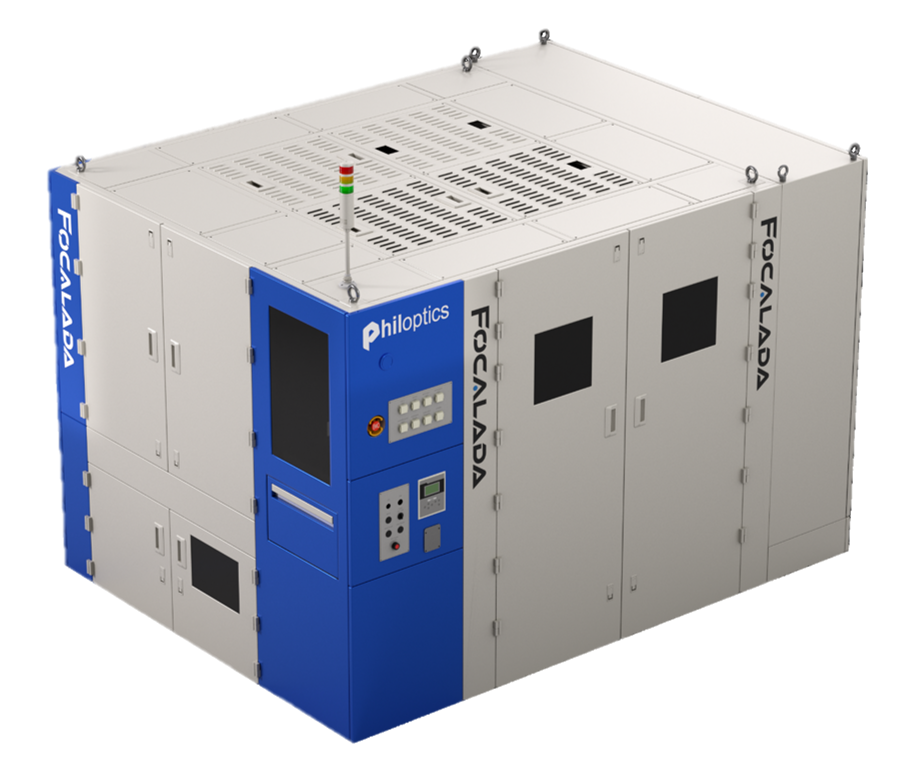
Total Hole 2.5D Image 처리 기술
AI 딥러닝을 통한 자동 결함 분류 기술
Big Data 고속 병렬 처리 기술
~510x515㎜
≥ø10㎛
≤2.0t
· Location : ≥±3㎛
· Measurement : ≥±3㎛
· Defects : ≥10㎛
≤18min (Grab + Inspection)
Location, Size, Circularity, Defects
· Top to Bottom hole simultaneous measurement
· Deep learning based defect classification
· Process status feedback