

TGV AOI
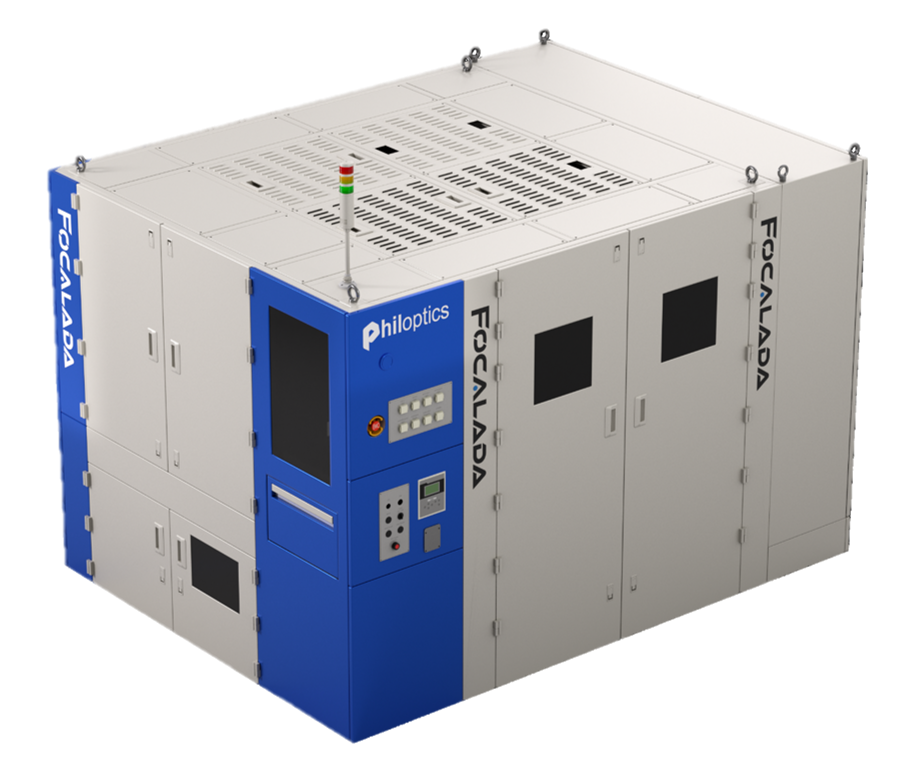
TGV孔及玻璃内部可视化与检测技术
基于AI深度学习的缺陷自动分类技术
大数据高速并行处理技术
~510x515㎜
≥ø10㎛
≤2.0t
· Location : ≥±3㎛
· Measurement : ≥±3㎛
· Defects : ≥10㎛
≤18min (Grab + Inspection)
Location, Size, Circularity, Defects
· Top to Bottom hole simultaneous measurement
· Deep learning based defect classification
· Process status feedback