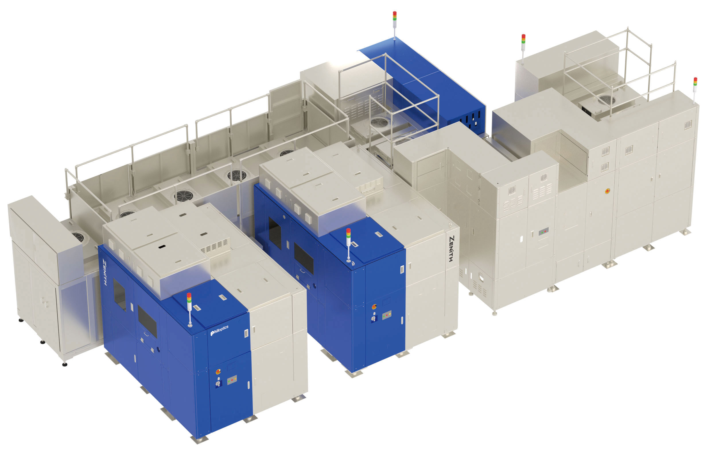

The TGV equip. is a high speed/precision processing Laser equipment that creates modifications on glass core substrates in the Adv.PKG process. After chemical etching, glass structuring (via holes & cavities, etc.) can be formed on the glass core substrate.
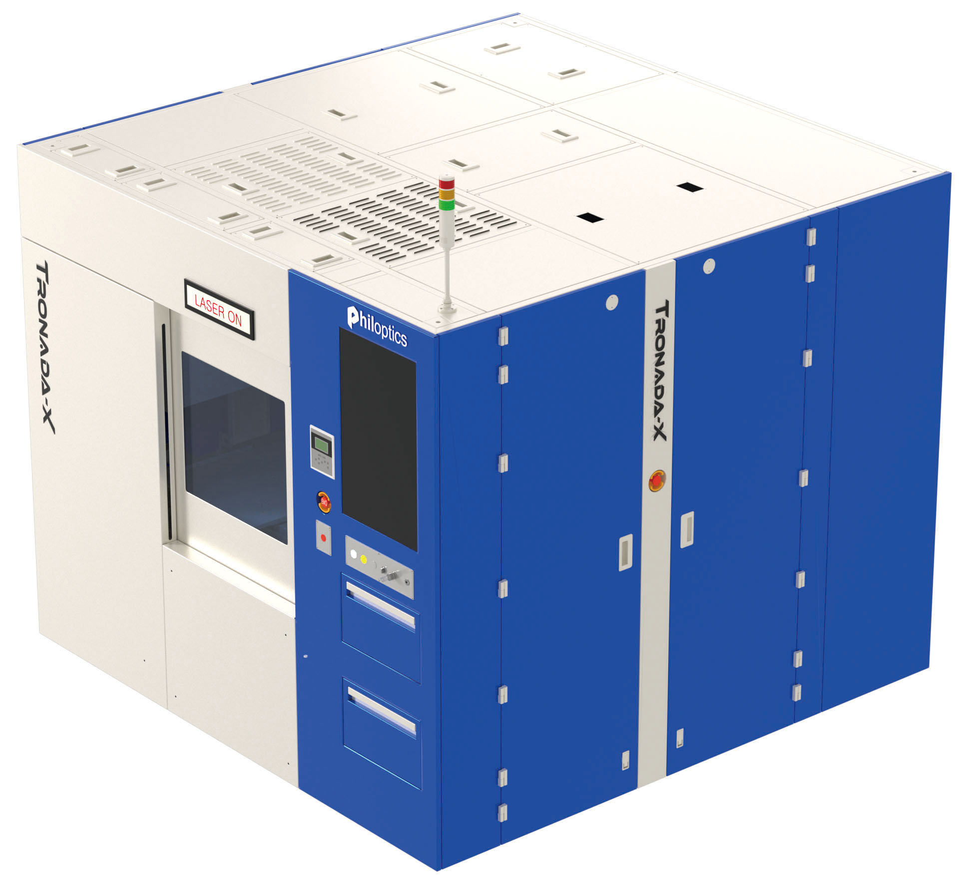
TGV AOI uses high-resolution, 2.5D imaging technology to accurately visualize and inspect TGV holes and internal glass structures. The system features GPU-based parallel processing capable of analyzing millions of holes in real time. It also has defect classification based on deep learning and automatic position correction, as well as user-customizable report output functions. These features enable an effective response to large-area, high-speed inspections and process optimization.
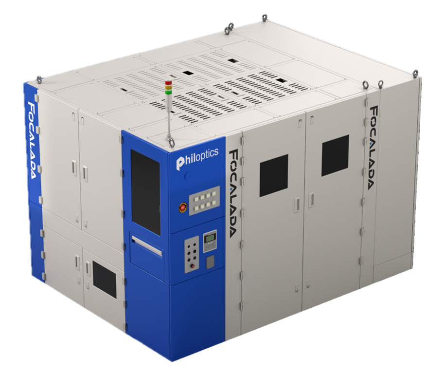
The ABF Via-Drilling equip. is a precision equipment for processing fine via holes in ABF with a UV laser in the Adv. PKG process. It can minimize the defect rate by monitoring the processing quality in real time when processing fine holes.
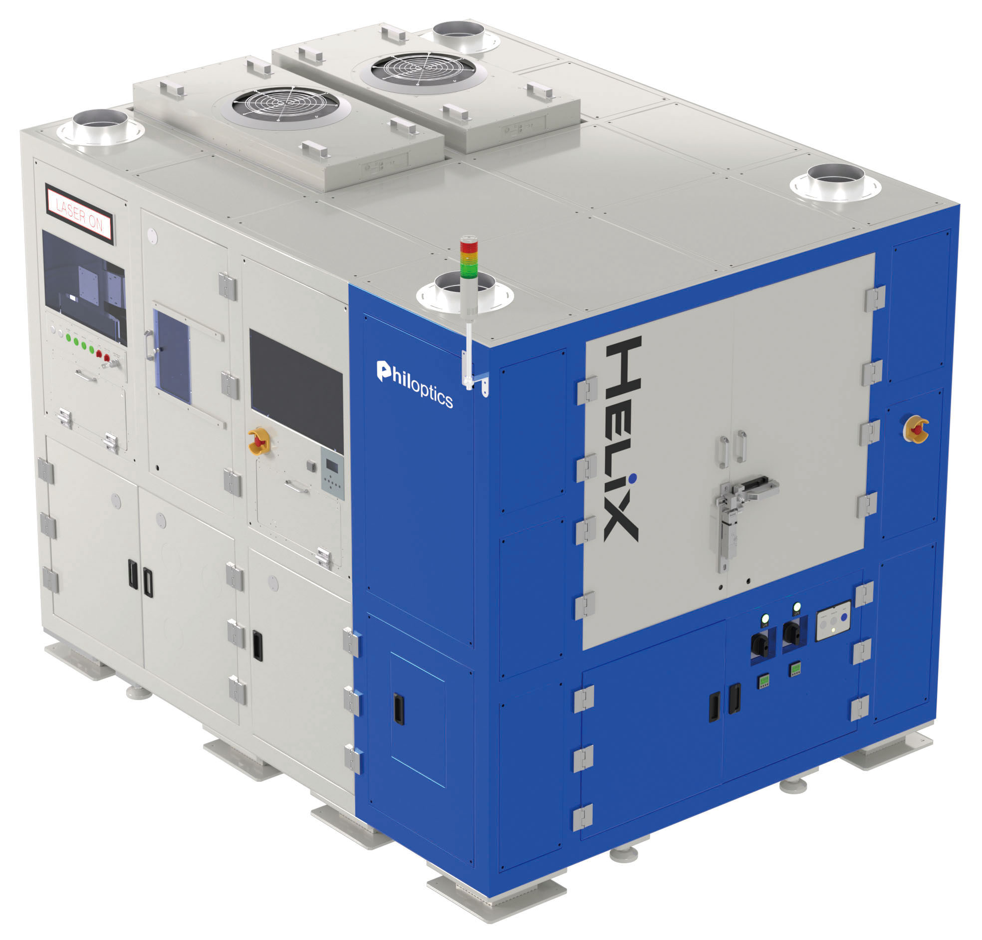
The DI exposure is a Direct Imaging equipment for circuit formation and SRO of solder resist in semiconductor and PCB processes using multiwavelength LEDs. It uses vision alignment without mask to improve positioning accuracy.
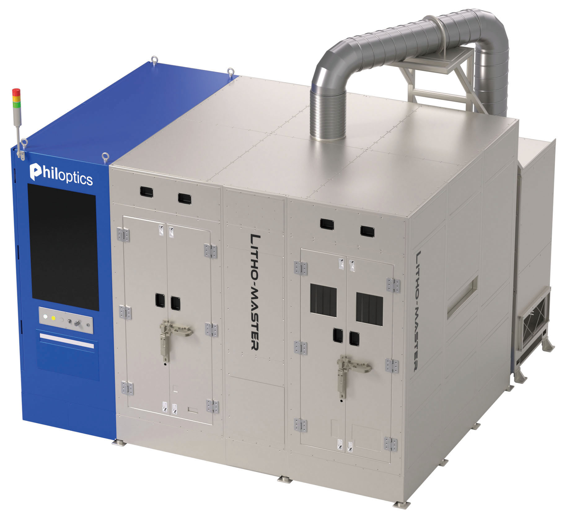
The advanced laser processing system revolutionizes glass substrate separation in the advanced packaging process, integrating EFEM, ablation, perforation, breaking, and sorting modules. Utilizing ultrashort pulse lasers and advanced scanning optics achieves the highest quality and speed in separating individual units from entire panels. This innovative solution sets new standards for high-precision, highthroughput manufacturing for next-generation microelectronics.